AD9929 データシートの表示(PDF) - Analog Devices
部品番号
コンポーネント説明
メーカー
AD9929 Datasheet PDF : 64 Pages
| |||
AD9929
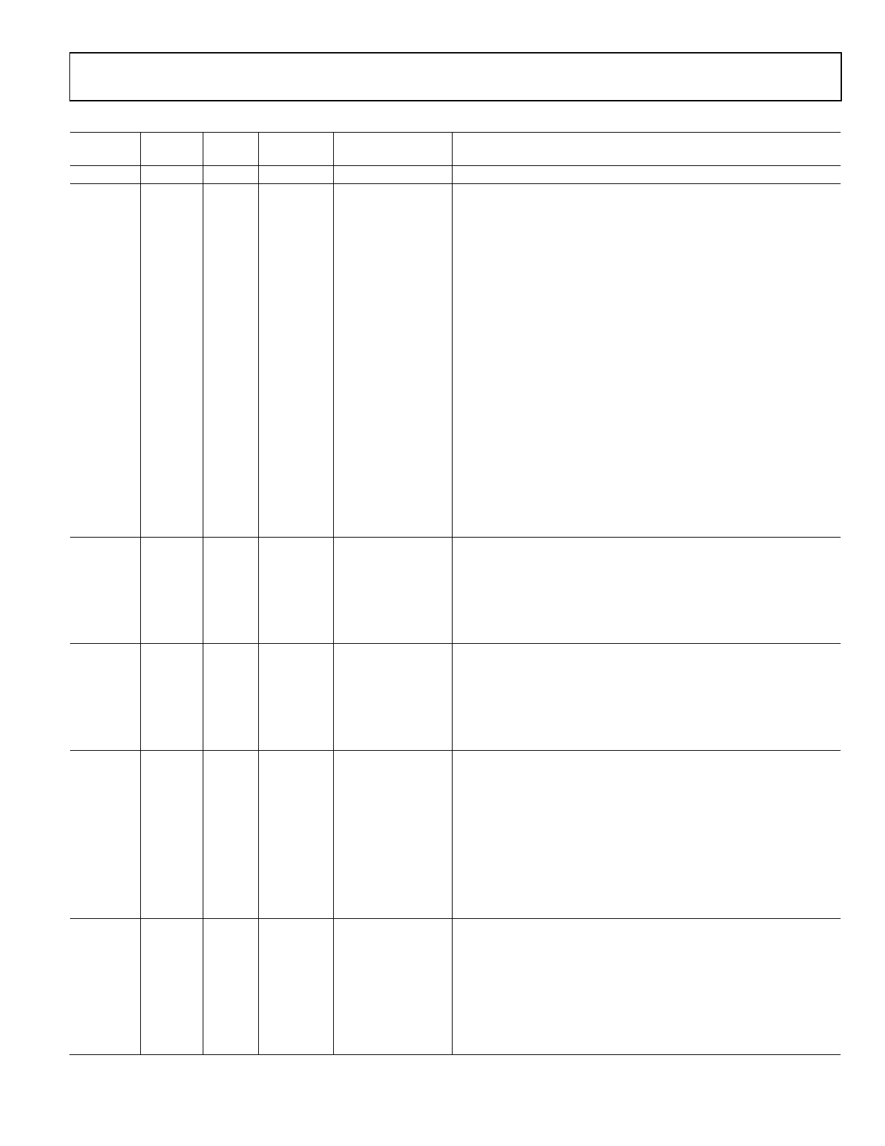
Table 8. Control Register Address Map
Bit
Default
Address Content Width Value
0x00
(23:0) 24
000000
0x01
23
1
0
(22:21) 2
(20:18) 3
0
17
1
1
16
1
0
(15:14) 2
0
13
1
0
(12:10) 3
0
(9:8)
2
0
0x02
0x03
0x04
0x05
7
1
6
1
5
1
4
1
(3:1)
3
0
1
(23:22) 2
(21:16) 6
(15:14) 2
(13:8) 6
(7:6)
2
(5:0)
6
(23:17) 7
16
1
(15:14) 2
(13:8) 6
(7:6)
2
(5:0)
6
(23:16) 8
15
1
(14:12) 3
11
1
(10:8) 3
(7:3)
5
(2:0)
3
(23:10) 14
9
1
8
1
(7:2)
6
1
1
0
0
1
1
0
0
0
0x34
0
0x18
0
0x0B
0x00
0
0
0x00
0
0x10
0x80
–
5
0
5
0x00
2
0x0000
0
0
00
0
0
1
1
Register Name
SW_RESET
Unused
XSUBCKSUPPRESS
Unused
HBLKMASK
SYNCPOL
Unused
XSUBCKMODE_HP
Unused
MSHUTPAT
MSHUT/VGATE_EN
Unused
CLPOB_CONT
CLPOB_MODE
Unused
VDMODE
Unused
SHDLOC
Unused
SHPLOC
DCLKPHASE
DOUTPHASE
Unused
H1BLKRETIME
Unused
H1POSLOC
Unused
RGNEGLOC
REFBLACK
Unused
H2DRV
Unused
H1DRV
Unused
RGDRV
Unused
AFESTBY
DIGSTBY
Unused
OUTCONT_REG
OUTCONT_ENB
Register Description
Software Reset = 000000 (Reset All Registers to Default )
Suppress XSUBCK (00 = No Suppression, 01 = Suppress First XSUBCK
After Last VSG Line Pulse, 10 = Suppress All XSUBCKs, Except Final
XSUBCK, 11 = No Suppression)
Test Mode. Should Be Set = 0
Masking Polarity for H1 During Blanking Period (0 = Low, 1 = High)
External SYNC Active Polarity (0 = Active Low)
High Precision Shutter Mode Operation
(0 = Single Pulse, 1 = Multiple Pulse)
Selects MSHUT Pattern. (See Figure 51)
(0 = Mshutpat0,1 = Mshutpat1,2 = Mshutpat2, 3 = Mshutpat3)
MSHUT Masking of VGATE Input (0 = MSHUT Does Not Mask VGATE,
1 = MSHUT Does Mask VGATE)
CLPOB Control (0 = CLPOB Off, 1 = CLPOB On)
CLPOB CCD Region Control (See Table 19)
VD Synchronous/Asynchronous Mode Setting
(0 = VD Synchronous, 1 = VD Asynchronous )
SHD Sample Location
SHP Sample Location
DCLK Pulse Adjustment
Data Output [11:0] Phase Adjustment
Retimes the H1 HBLK to Internal Clock
H1 Positive Edge Location
RG Negative Edge Location
Black Level Clamp
H2 Drive Strength (0 = Off, 1 = 4.3 mA, 2 = 8.6 mA, 3 = 12.9 mA,
4 = 17.2 mA, 5 = 21.5 mA, 6 = 25.8 mA, 7 = 30.1 mA)
H1 Drive Strength (0 = Off, 1 = 4.3 mA, 2 = 8.6 mA, 3 = 12.9 mA,
4 = 17.2 mA, 5 = 21.5 mA, 6 = 25.8 mA, 7 = 30.1 mA)
RG Drive Strength (0 = Off, 1 = 2.15 mA, 2 = 4.2 mA, 3 = 6.45 mA,
4 = 8.6 mA, 5 = 10.75 mA, 6 = 12.9 mA, 7 = 15.05 mA)
AFE Standby (0 = Standby, 1 = Normal Operation)
Digital Standby (0 = Standby, 1 = Normal Operation)
Internal OUTCONT Signal Control
(0 = Digital Outputs Held at Fixed DC Level, 1 = Normal Operation)
External OUTCONT Signal Input Pin 43 Control (0 = Pin Enabled,
1 = Pin Disabled)
Rev. A | Page 11 of 64
Share Link: 