CS61582 データシートの表示(PDF) - Cirrus Logic
部品番号
コンポーネント説明
メーカー
CS61582 Datasheet PDF : 32 Pages
| |||
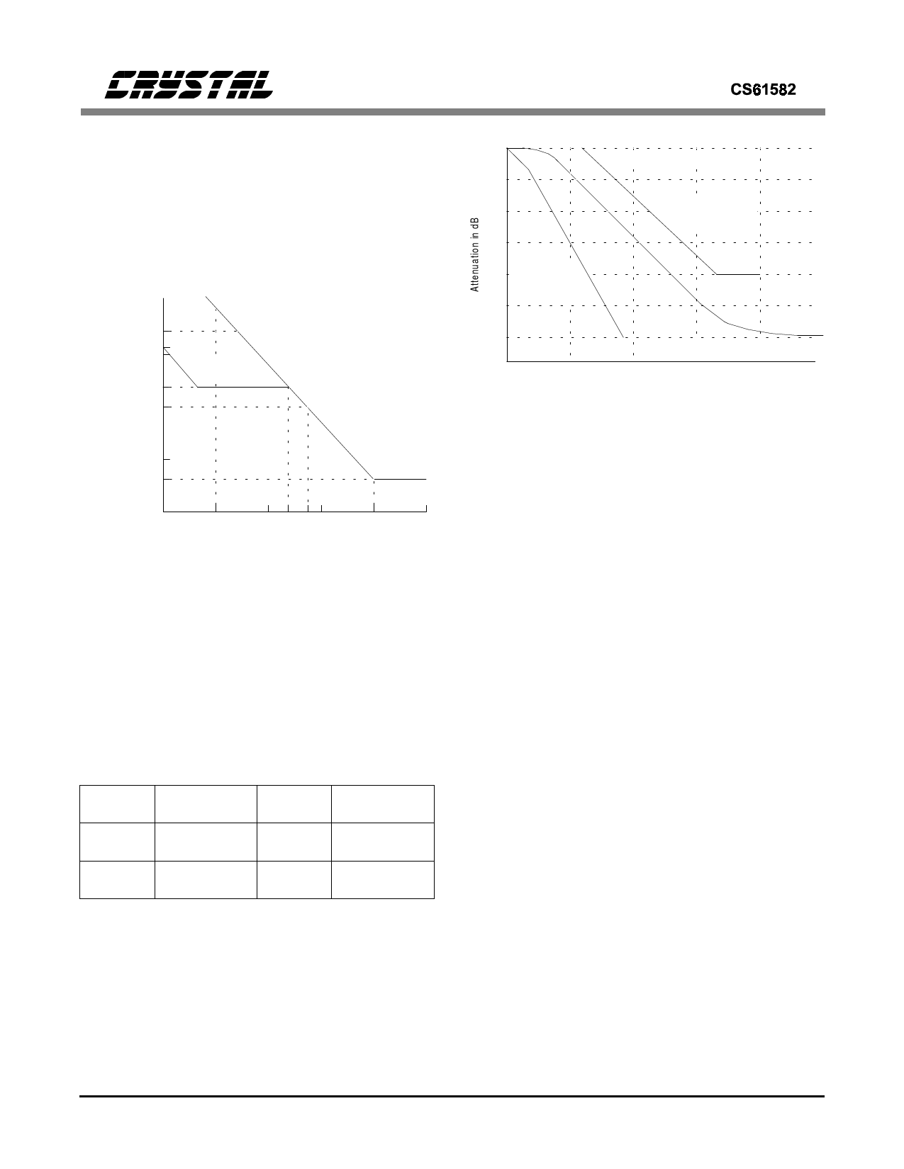
The clock recovery circuit is a second-order
phase locked loop that can tolerate up to 0.4 UI
of jitter from 10 kHz to 100 kHz without gener-
ating errors (Figure 7). The clock and data
recovery circuit is tolerant of long strings of con-
secutive zeros and will successfully recover a
1-in-175 jitter-free line input signal.
300
138
100
28
P E A K -T O -P E A K
JITTER
10
(unit intervals)
CS61582
P e rfo rm a n c e
AT&T 62411
(1990 Version)
1
.4
.1
1
10
100 300 700 1k
10k
100k
JITTER FREQUENCY (Hz)
Figure 7. Minimum Input Jitter Tolerance of Receiver
Recovered data at RPOS and RNEG is stable
and may be sampled using the recovered clock
RCLK. The CLKE input determines the clock
polarity where the output data is stable and valid
as shown in Table 2. When CLKE is low, RPOS
and RNEG are valid on the rising edge of
RCLK. When CLKE is high, RPOS and RNEG
are valid on the falling edge of RCLK.
CLKE
LOW
HIGH
DATA
RPOS
RNEG
RPOS
RNEG
CLOCK
RCLK
RCLK
RCLK
RCLK
Clock Edge
for Valid Data
Rising
Rising
Falling
Falling
Table 2. Recovered Data/Clock Options
JITTER ATTENUATOR
The jitter attenuator is located in the transmit
path of each channel to remove gapped clock jit-
ter on TCLK. Figure 8 illustrates the typical
jitter attenuation curve.
DS224PP1
0
10
20
30
40 b) Maximum
A tte n u a tio n
Lim it
50
a) M inimum Attenuation Lim it
62411 (1990 Version)
Requirem ents
60
CS61582 Performance
1
10
100
1k
10 k
Frequency in Hz
Figure 8. Typical Jitter Transfer Function
The attenuator consists of a 64-bit FIFO, a nar-
row-band monolithic PLL, and control logic.
Signal jitter is absorbed in the FIFO which is de-
signed to neither overflow nor underflow. If
overflow or underflow is imminent, the jitter
transfer function is altered to insure that no bit-
errors occur. Under this condition, jitter gain
may occur and jitter should be attenuated exter-
nally in a frame buffer. The jitter attenuator will
typically tolerate 43 UIs before the overflow/un-
derflow mechanism occurs. If the jitter
attenuator has not had time to "lock" to the aver-
age incoming frequency (e.g., following a device
reset) the attenuator will tolerate a minimum of
22 UIs before the overflow/underflow mecha-
nism occurs. The attenuator can accept a
transmit clock with gaps ≤ 28 UIs and a transmit
clock burst rate of ≤ 8 MHz.
When a loss of signal occurs, the last recovered
frequency is not held and the output frequency be-
comes the frequency of the reference clock.
REFERENCE CLOCK
The CS61582 requires a reference clock with a
minimum accuracy of ±100 ppm for T1 and E1
applications. This clock can be either a 1X clock
(i.e., 1.544 MHz or 2.048 MHz), or can be a 8X
clock (i.e., 12.352 MHz or 16.384 MHz) as se-
11
Share Link: 