CS61583 データシートの表示(PDF) - Cirrus Logic
部品番号
コンポーネント説明
メーカー
CS61583 Datasheet PDF : 44 Pages
| |||
CS61583
age incoming frequency (e.g. following a device
reset) the attenuator will tolerate a minimum of
22 UIs before the overflow/underflow mecha-
nism occurs.
For T1/E1 line cards used in high-speed muti-
plexers (e.g., SONET and SDH), the jitter
attenuator is typically used in the transmit path.
The attenuator can accept a transmit clock with
gaps ≤ 28 UIs and a transmit clock burst rate of
≤ 8 MHz.
When the jitter attenuator is in the receive path and
loss of signal occurs, the frequency of the last re-
covered signal is held. When the jitter attenuator is
not in the receive path, the last recovered frequency
is not held and the output frequency becomes the
frequency of the reference clock.
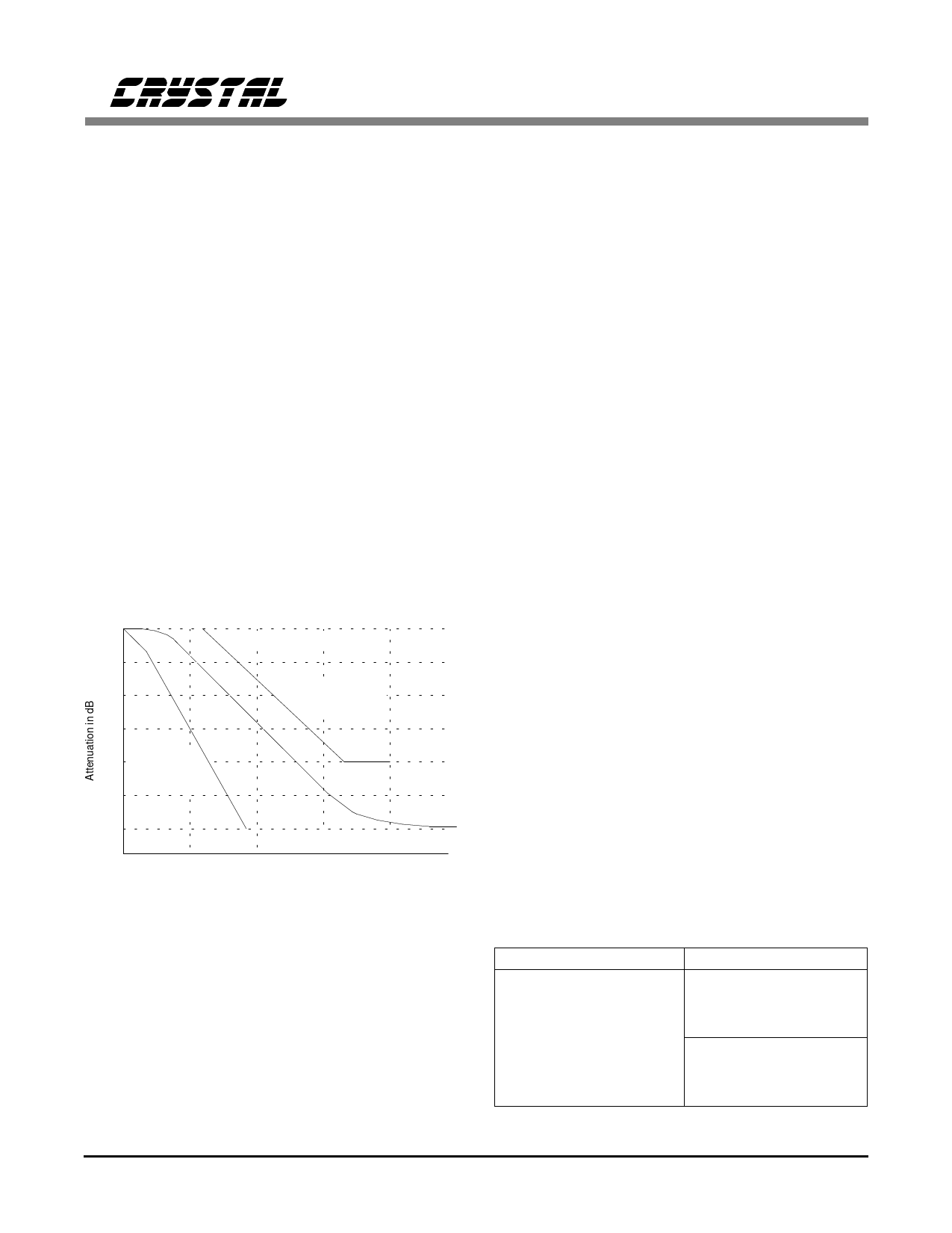
A typical jitter attenuation curve is shown in Fig-
ure 9.
0
10
20
30
40 b) Maximum
Attenuation
Limit
50
a) Minimum Attenuation Limit
62411 (1990 Version)
Requirements
60
1
CS61583 Performance
10
100
1k
10 k
Frequency in Hz
Figure 9. Typical Jitter Transfer Function
REFERENCE CLOCK
The CS61583 requires a reference clock with a
minimum accuracy of ±100 ppm for T1 and E1
applications. This clock can be either a 1X clock
(i.e., 1.544 MHz or 2.048 MHz), or can be a 8X
clock (i.e., 12.352 MHz or 16.384 MHz) as se-
lected by the 1XCLK pin. In systems with a
DS172PP5
jittered transmit clock, the reference clock
should not be tied to the transmit clock and a
separate external oscillator should drive the ref-
erence clock input. Any jitter present on the
reference clock will not be filtered by the jitter
attenuator.
POWER-UP RESET
On power-up, the device is held in a static state
until the power supply achieves approximately
60% of the power supply voltage. When this
threshold is crossed, the device waits another 10
ms to allow the power supply to reach operating
voltage and then calibrates the transmit and re-
ceive circuitry. This initial calibration takes less
than 20 ms but can occur only if REFCLK and
TCLK are present. The power-up reset performs
the same functions as the RESET pin.
LINE CONTROL AND MONITORING
Line control and monitoring of the CS61583 is
achieved using the control pins. The controls and
indications available on the CS61583 are de-
tailed below.
Line Code Encoder/Decoder
Coding may be transparent, AMI, B8ZS, or
HDB3 and is selected using the CODER1,
CODER2, AMI1, and AMI2 pins. In the coder
mode, AMI, B8ZS, and HDB3 line codes are
available. The input data to the encoder is on
TDATA and the output data from the decoder is
in NRZ format on RDATA. See Table 4.
CODER[2:1]=0
Transparent Mode
Enabled
and
AMI[2:1] Pin(s)
Disabled
CODER[2:1]=1
AMI[2:1]=0
B8ZS/HDB3
Encoder/Decoder
Enabled
AMI[2:1]=1
AMI
Encoder/Decoder
Enabled
Table 4. Coder Mode Options
13
Share Link: 