CS61583 データシートの表示(PDF) - Cirrus Logic
部品番号
コンポーネント説明
メーカー
CS61583 Datasheet PDF : 44 Pages
| |||
CS61583
receive circuitry is calibrated if REFCLK and shift operation. Note that if J-TDI is floating,
TCLK are present.
an internal pull-up resistor forces the pin high.
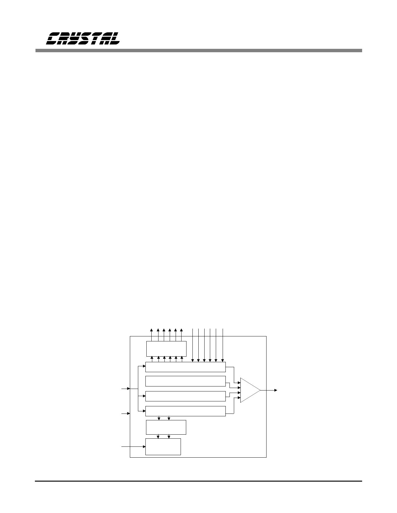
JTAG BOUNDARY SCAN
Board testing is supported through JTAG bound-
ary scan. Using boundary scan, the integrity of
the digital paths between devices on a circuit
board can be verified. This verification is sup-
ported by the ability to externally set the signals
on the digital output pins of the CS61583, and to
externally read the signals present on the input
pins of the CS61583. Additionally, the manufac-
turer ID, part number and revision of the
CS61583 can be read during board test using
JTAG boundary scan.
As shown in Figure 10, the JTAG hardware con-
sists of data and instruction registers plus a Test
Access Port (TAP) controller. Control of the TAP
is achieved through signals applied to the Test
Mode Select (J-TMS) and Test Clock ( J-TCK)
input pins. Data is shifted into the registers via
the Test Data Input (J-TDI) pin, and shifted out
of the registers via the Test Data Output (J-TDO)
pin. Both J-TDI and J-TDO are clocked at a rate
determined by J-TCK. The Instruction register
defines which data register is accessed in the
JTAG Data Registers (DR)
The test data registers are the Boundary-Scan
Register (BSR), the Device Identification Regis-
ter (DIR), and the Bypass Register (BR).
Boundary Scan Register: The BSR is connected
in parallel to all the digital I/O pins, and pro-
vides the mechanism for applying/reading test
patterns to/from the board traces. The BSR is 67
bits long and is initialized and read using the in-
struction SAMPLE/PRELOAD. The bit ordering
for the BSR is the same as the top-view package
pin out, beginning with the LOS1 pin and mov-
ing counter-clockwise to end with the CODER1
pin as shown in Table 5. Note that the analog,
oscillator, power, ground, CLKE, and ATTEN0
pins are not included as part of the boundary-
scan register.
The input pins require one bit in the BSR and
only one J-TCK cycle is required to load test
data for each input pin.
The output pins have two bits in the BSR to de-
fine output high, output low, or high impedance.
Digital output pins Digital input pins
J-TDI
J-TCK
J-TMS
parallel latched
output
Boundary Scan Data Register
Device ID Data Register
Bypass Data Register
Instruction (shift) Register
parallel latched
output
TAP
Controller
JTAG Block
MUX
J-TDO
Figure 10. Block Diagram of JTAG Circuitry
DS172PP5
15
Share Link: 