LTC1742IFW データシートの表示(PDF) - Linear Technology
部品番号
コンポーネント説明
メーカー
LTC1742IFW Datasheet PDF : 20 Pages
| |||
LTC1742
APPLICATIO S I FOR ATIO
Spurious Free Dynamic Range (SFDR)
Spurious free dynamic range is the peak harmonic or
spurious noise that is the largest spectral component
excluding the input signal and DC. This value is expressed
in decibels relative to the RMS value of a full scale input
signal.
Input Bandwidth
The input bandwidth is that input frequency at which the
amplitude of the reconstructed fundamental is reduced by
3dB for a full scale input signal.
Aperture Delay Time
The time from when a rising ENC equals the ENC voltage
to the instant that the input signal is held by the sample and
hold circuit.
Aperture Delay Jitter
The variation in the aperture delay time from conversion to
conversion. This random variation will result in noise
when sampling an AC input. The signal to noise ratio due
to the jitter alone will be:
SNRJITTER = –20log (2π) • FIN • TJITTER
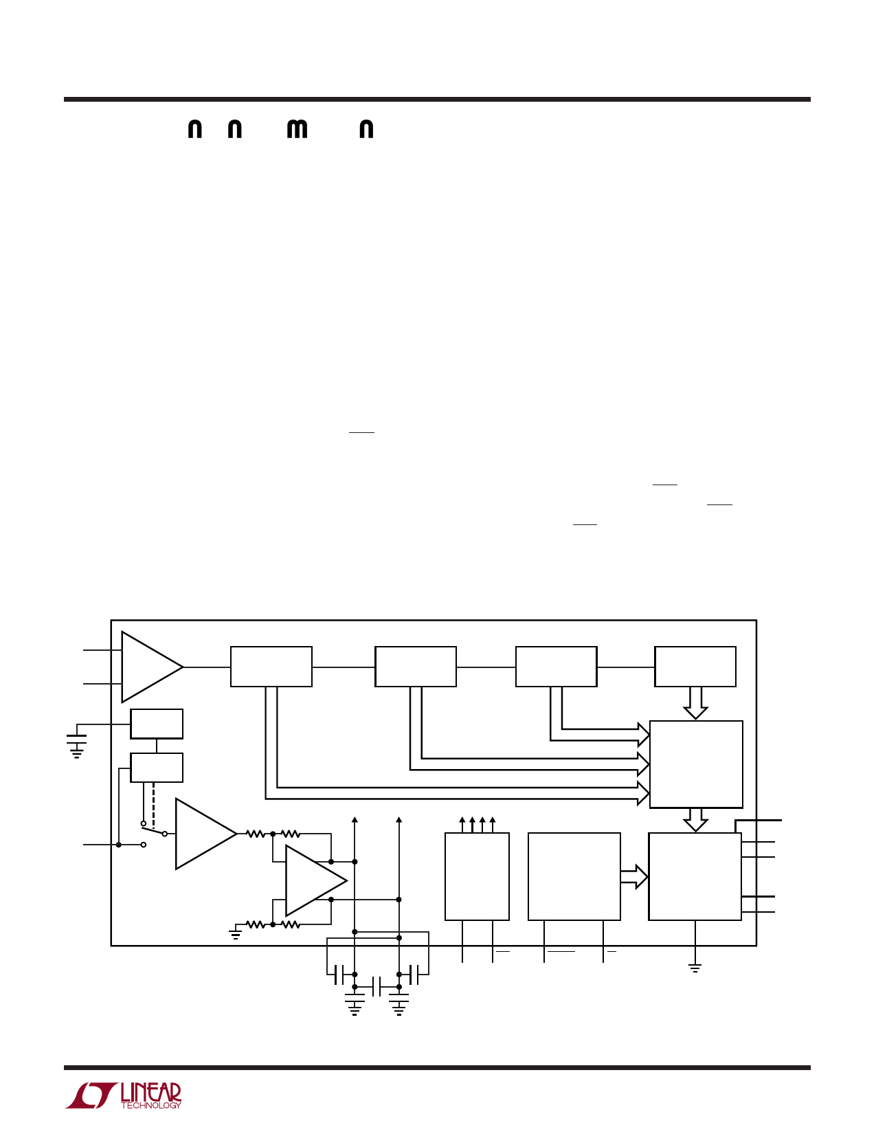
CONVERTER OPERATION
The LTC1742 is a CMOS pipelined multistep converter.
The converter has four pipelined ADC stages; a sampled
analog input will result in a digitized value five cycles later,
see the Timing Diagram section. The analog input is
differential for improved common mode noise immunity
and to maximize the input range. Additionally, the differen-
tial input drive will reduce even order harmonics of the
sample-and-hold circuit. The encode input is also
differential for improved common mode noise immunity.
The LTC1742 has two phases of operation, determined by
the state of the differential ENC/ENC input pins. For brev-
ity, the text will refer to ENC greater than ENC as ENC high
and ENC less than ENC as ENC low.
Each pipelined stage shown in Figure 1 contains an ADC,
a reconstruction DAC and an interstage residue amplifier.
AIN+
INPUT
AIN–
S/H
VCM
4.7µF
2.35V
REFERENCE
RANGE
SELECT
REF
SENSE
BUF
FIRST PIPELINED
ADC STAGE
(5 BITS)
DIFF
REF
AMP
SECOND PIPELINED
ADC STAGE
(4 BITS)
THIRD PIPELINED
ADC STAGE
(4 BITS)
REFL
REFH INTERNAL CLOCK SIGNALS
DIFFERENTIAL
INPUT
LOW JITTER
CLOCK
DRIVER
CONTROL LOGIC
AND
CALIBRATION LOGIC
REFLB REFHA REFLA REFHB ENC ENC
0.1µF
4.7µF
0.1µF
1µF
1µF
MSBINV
OE
Figure 1. Functional Block Diagram
FOURTH PIPELINED
ADC STAGE
(4 BITS)
SHIFT REGISTER
AND CORRECTION
OUTPUT
DRIVERS
OVDD 0.5V TO
5V
OF
D13
D0
CLKOUT
OGND
1742 F01
1742f
11
Share Link: 