M7040N データシートの表示(PDF) - STMicroelectronics
部品番号
コンポーネント説明
メーカー
M7040N Datasheet PDF : 159 Pages
| |||
M7040N
Full In (FULI[6:0]). Each signal in this bus is con-
nected to FULO[0] or FULO[1] of an upstream de-
vice to generate the FULL signal for the depth-
cascaded block. For more information, see
DEPTH-CASCADING, page 124 to Generate Full
for a Block Section.
Full Out (FULO[1:0]). FULO[1] and FULO[0] are
the same logical signal. One of these two signals
must be connected to the FULI of up to four down-
stream devices in a depth-cascaded table. Bit [0]
in the data array indicates if the entry is full (1) or
empty (0).This signal is asserted if all of the bits in
the data array are '1s.' Refer to Depth-Cascading
to Generate a “FULL” Signal, page 124.
Full Flag (FULL). When asserted, this signal in-
dicates that the table consisting of many depth-
cascaded devices is full.
Device Identification (ID[4:0]). The binary-en-
coded device ID for a depth-cascaded system
starts at 00000 and goes up to 11110. 11111 is re-
served for a special broadcast address that se-
lects all cascaded search engines in the system.
On a broadcast read-only, the device with the
LDEV bit set to '1' responds.
Chip Core Supply (VDD). This is equal to 1.5V.
Chip I/O Supply (VDDQ). This is equal to either
2.5 or 3.3V.
Test Data In (TDI). This is the Test Access Port’s
Test Data In.
Test Clock (TCK). This is the Test Access Port’s
Test Clock.
Test Data Out (TDO). This is the Test Access
Port’s Test Data Out.
Test Mode Select (TMS). This is the Test Ac-
cess Port’s Test Mode Select.
Test Reset (TRST_L). This is the Test Access
Port’s Test Reset.
CLOCKS
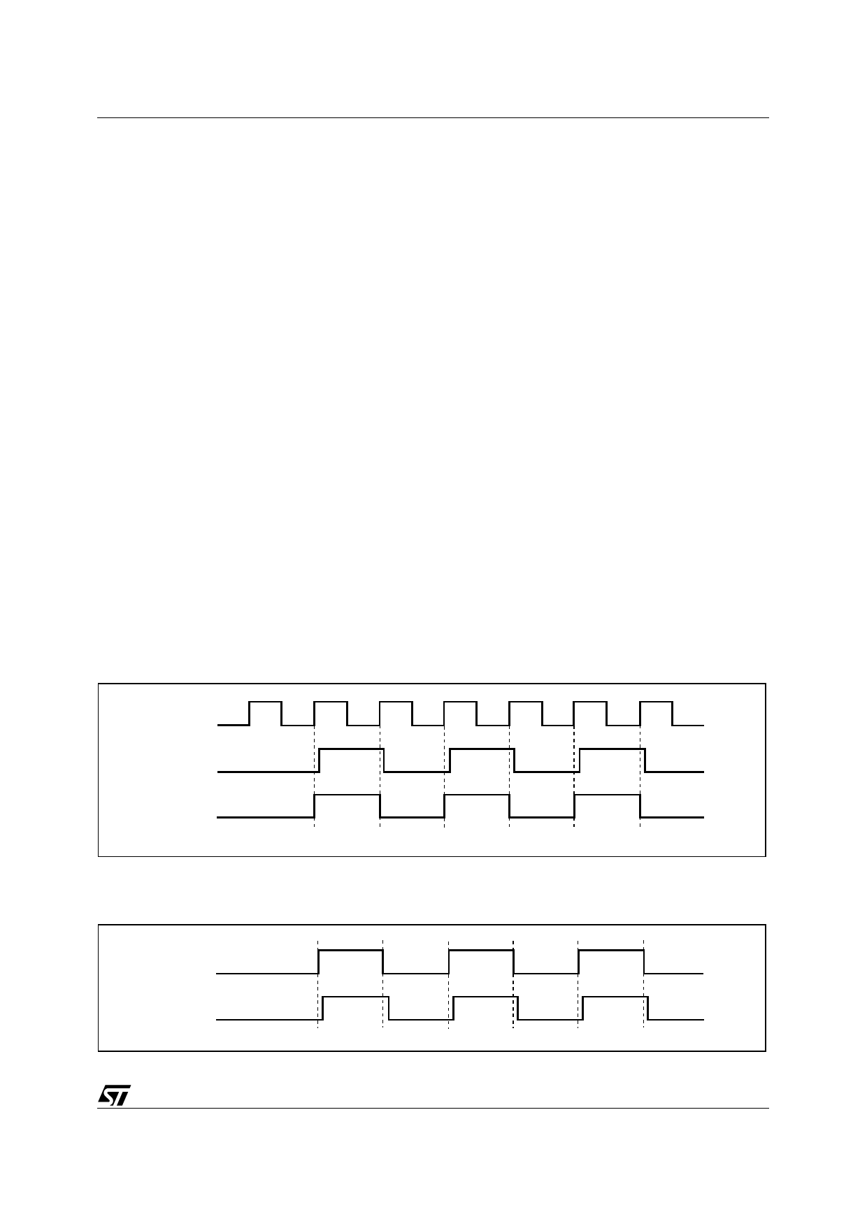
If the CLK_MODE pin is low, M7040N receives the
CLK2X and PHS_L signals. It uses the PHS_L sig-
nal to divide CLK2X and generate an internal clock
(CLK), as shown in Figure 10. The M7040N uses
CLK2X and CLK for internal operations. If the
CLK_MODE pin is high, the M7040N receives the
CLK1X only. the M7040N uses an internal PLL to
double the frequency of CLK1X and then divides
Figure 10. Clocks (CLK2X and PHS_L)
that clock by two to generate a CLK for internal op-
erations, as shown in Figure 11.
Note: For the purpose of showing timing dia-
grams, all such diagrams in this document will be
shown in CLK2X mode. For a timing diagram in
CLK1X mode, the following substitution can be
made (see Figure 12).
CLK2X
P HS_L
CLK(1)
Note: Any reference to “CLK Cycles” means 1 cycle of the signal, “CLK.”
1. “CLK” is an internal signal.
Figure 11. Clocks (CLK1X)
AI04750
CLK1X
CLK(1)
1. “CLK” is an internal signal.
AI04665
21/159
Share Link: 