SST49LF004B データシートの表示(PDF) - Silicon Storage Technology
部品番号
コンポーネント説明
メーカー
SST49LF004B Datasheet PDF : 36 Pages
| |||
4 Mbit Firmware Hub
SST49LF004B
MODE SELECTION
The SST49LF004B flash memory device operates in two
distinct interface modes: the LPC mode and the Parallel
Programming (PP) mode. The MODE (Interface Mode
Select) pin is used to set the interface mode selection. If the
MODE pin is set to logic high, the device is in PP mode;
while if the MODE pin is set low, the device is in LPC mode.
The MODE selection pin must be configured prior to device
operation and must not change during operation. If the pin
is not connected, by default the Mode pin is internally
pulled low and the 49LF00xB will be in LPC operation.
In LPC mode, communication between the Host and the
SST49LF004B occurs via the 4-bit I/O communication sig-
nals, LAD[3:0] and LFRAME#. The SST49LF004B detects
whether it is being accessed via a FWH Read or FWH
Write cycle by detecting the START field contents; 91101b
is a FWH read cycle and a 1110b indicates a FWH Write
cycle.
In PP mode, the device is controlled via the 11 addresses,
A10-A0, and 8 I/O, DQ7-DQ0, signals. The address inputs
are multiplexed in row and column selected by control sig-
nal R/C# pin. The row addresses are mapped to the lower
internal addresses (A10-0), and the column addresses are
mapped to the higher internal addresses (A18-11). See Fig-
ure 3, Device Memory Map, for address assignments.
LPC MODE
EOL Data Sheet
Device Operation
The LPC mode uses a 5-signal communication interface
consisting of one control line, LFRAME#, which is driven by
the host to start or abort a bus cycle, and a 4-bit data bus,
LAD[3:0], which is used to communicate cycle type, cycle
direction, ID selection, address, data and sync fields. The
device enters standby mode when LFRAME# is high and
no internal operation is in progress.
The SST49LF004B supports single-byte Firmware Mem-
ory Read/Write cycles as defined in Intel’s Low-Pin-Count
Interface Specification. The host drives LFRAME# low for
one or more clock cycles to initiate an LPC cycle. The last
latched value of LAD[3:0] before LFRAME# is the START
value. The START value determines whether the
SST49LF004B will respond to a Firmware Memory Read
or Firmware Memory Write cycle as defined in Table 3.
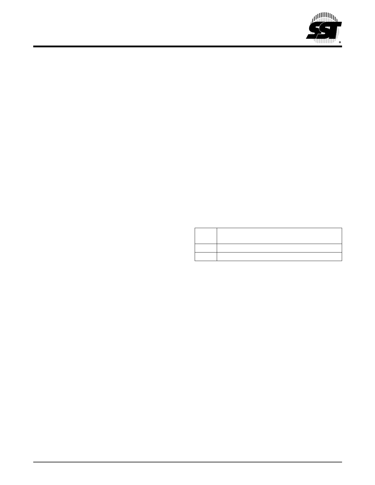
TABLE 3: FIRMWARE MEMORY CYCLES START
FIELD DEFINITION
START
Value Definition
1101 Start of a Firmware Memory Read cycle
1110 Start of a Firmware Memory Write cycle
T3.0 1307
See following sections for details of Firmware Memory
cycle types. JEDEC standard SDP (Software Data Protec-
tion) Program and Erase command sequences are used
to initiate Firmware Memory Program and Erase opera-
tions. See Table 9 for a listing of Program and Erase com-
mands. Chip-Erase is only available in PP mode.
©2007 Silicon Storage Technology, Inc.
11
S71307-03-EOL
12/07
Share Link: 