CXD3503R データシートの表示(PDF) - Sony Semiconductor
部品番号
コンポーネント説明
メーカー
CXD3503R Datasheet PDF : 19 Pages
| |||
CXD3503R
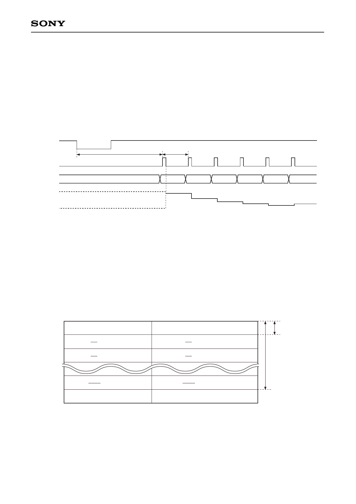
Description of Output Correction Signal Operation
Horizontal direction
The correction data set in the SRAM by serial transfer is arithmetically processed inside the IC to determine
the output position corresponding to the value set by serial register HP7 to 0 using the front edge of HSYNC as
the reference. Interpolation is not performed for the horizontal direction, and interpolated data is output at the
cycle set by serial register HINT7 to 0 for the vertical direction. In addition, the maximum amplitude of the
correction signal output voltage is determined by VRH (Pin 44) and VRL (Pin 40). The internal DAC outputs at
the resistive potential division (VRH to VRL: 213Ω typ.), so be sure to input to VRH and VRL via buffers having
current capacity.
HSYNC
DACKO/I
Set by HP7 to 0
Set by HINT7 to 0
DOUT
VRH
DACO
VRL
The internally generated digital data DOUT is input to the internal D/A converter, latched by the D/A converter
clock input from DACKI, and output from DACO2, 1 and 0 as an analog signal.
Note) If edges remain, these level differences may appear as vertical stripes. Therefore, when using this as a
correction signal, be sure to eliminate the edges using an LPF, etc. before input to the CXA2111R or
CXA2112R.
Vertical direction
The vertical correction points set in the SRAM are arithmetically processed inside the IC to output interpolated
data for the lines other than correction points.
n
fm, n
m
fm, n +
1
a
(fm + 1, n – fm, n)
fm, n +
2
a
(fm + 1, n – fm, n)
n+1
fm + 1, n
fm, n + 1 +
1
a
(fm + 1, n + 1 – fm, n + 1)
fm, n + 1 +
2
a
(fm + 1, n + 1 – fm, n + 1)
VINT line(s)
a' lines
m+1
fm,
n
+
a–
a
1
(fm + 1,
n
–
fm,
n)
fm,
n
+
1
+
a
–
a
1
(fm
+
1,
n
+
1
–
fm,
n
+
1)
fm + 1, n
fm + 1, n + 1
fm, n: Correction data for point (m, n)
Vertical correction point interval
Set by VINT4 to 0 and ANM5 to 0
Assuming ANM5 to 0 = a,
a' = VINT × a
– 11 –
Share Link: 