CS61304A データシートの表示(PDF) - Cirrus Logic
部品番号
コンポーネント説明
メーカー
CS61304A Datasheet PDF : 32 Pages
| |||
RTIP
1:2
RRING
CS61304A
CS61304A
Data
Level
Slicer
Edge
Detector
Data
Sampling
&
Clock
Extraction
Clock
Phase
Selector
Jitter
Attenuator
RPOS
RNEG
RCLK
Continuously
Calibrated
Delay Line
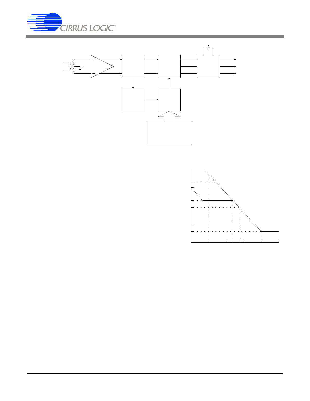
Figure 10. Receiver Block Diagram
put from the phase selector feeds the clock and
data recovery circuits which generate the recov-
ered clock and sample the incoming signal at
appropriate intervals to recover the data.
Data sampling will continue at the periods se-
lected by the phase selector until an incoming
pulse deviates enough to cause a new phase to be
selected for data sampling. The phases of the de-
lay line are selected and updated to allow as much
as 0.4 UI of jitter from 10 kHz to 100 kHz, with-
out error. The jitter tolerance of the receiver
exceeds that shown in Figure 11. Additionally,
this method of clock and data recovery is tolerant
of long strings of consecutive zeros. The data
sampler will continuously sample data based on
its last input until a new pulse arrives to update
the clock phase selector.
The delay line is continuously calibrated using
the crystal oscillator reference clock. The delay
line produces 13 phases for each cycle of the ref-
erence clock. In effect, the 13 phases are
analogous to a 20 MHz clock when the reference
clock is 1.544 MHz. This implementation utilizes
the benefits of a 20 MHz clock for clock recovery
without actually having the clock present to im-
pede analog circuit performance.
300
138
100
28
10
PEAK-TO-PEAK
JITTER
(unit intervals)
1
.4
.1
1
Minimum
Performance
AT&T 62411
10
100 300 700 1k
10k
JITTER FREQUENCY (Hz)
100k
Figure 11. Minimum Input Jitter Tolerance of Receiver
(Clock Recovery Circuit and Jitter Attenuator)
In the Hardware Mode, data at RPOS and RNEG
should be sampled on the rising edge of RCLK,
the recovered clock. In the Extended Hardware
Mode, data at RDATA should be sampled on the
falling edge of RCLK. In the Host Mode, CLKE
determines the clock polarity for which output
data should be sampled as shown in Table 5.
12
DSD1S5165P6PF21
Share Link: 