CS61304A データシートの表示(PDF) - Cirrus Logic
部品番号
コンポーネント説明
メーカー
CS61304A Datasheet PDF : 32 Pages
| |||
CS61304A
CS61304A
In operation, the delay lines are continuously cali-
brated, making the performance of the device
independent of power supply or temperature vari-
ations. The continuous calibration function
forgoes any requirement to reset the line interface
when in operation. However, a reset function is
available which will clear all registers.
In the Hardware and Extended Hardware Modes,
a reset request is made by simultaneously setting
both the RLOOP and LLOOP pins high for at
least 200 ns. Reset will initiate on the falling edge
of the reset request (falling edge of RLOOP and
LLOOP). In the Host Mode, a reset is initiated by
simultaneously writing RLOOP and LLOOP to
the register. In either mode, a reset will set all reg-
isters to 0 and force the oscillator to its center
frequency before initiating calibration. A reset
will also set LOS high.
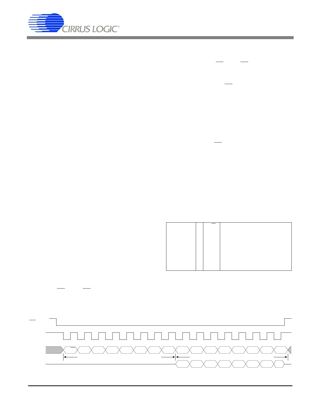
Serial Interface
In the Host Mode, pins 23 through 28 serve as a
microprocessor/microcontroller interface. One
on-board register can be written to via the SDI
pin or read from via the SDO pin at the clock rate
determined by SCLK. Through this register, a
host controller can be used to control operational
characteristics and monitor device status. The se-
rial port read/write timing is independent of the
system transmit and receive timing.
Data transfers are initiated by taking the chip se-
lect input, CS, low (CS must initially be high).
Address and input data bits are clocked in on the
rising edge of SCLK. The clock edge on which
output data is stable and valid is determined by
CLKE as shown in Table 5. Data transfers are ter-
minated by setting CS high. CS may go high no
sooner than 50 ns after the rising edge of the
SCLK cycle corresponding to the last write bit.
For a serial data read, CS may go high any time
to terminate the output.
Figure 13 shows the timing relationships for data
transfers when CLKE = 1. When CLKE = 1, data
bit D7 is held until the falling edge of the 16th
clock cycle. When CLKE = 0, data bit D7 is held
until the rising edge of the 17th clock cycle. SDO
goes High-Z after CS goes high or at the end of
the hold period of data bit D7.
An address/command byte, shown in Table 9, pre-
cedes a data register. The first bit of the
address/command byte determines whether a read
or a write is requested. The next six bits contain
the address. The line interface responds to address
16 (0010000). The last bit is ignored.
LSB, first bit
MSB, last bit
0 R/W Read/Write Select; 0 = write, 1 = read
1 ADD0 LSB of address, Must be 0
2 ADD1 Must be 0
3 ADD2 Must be 0
4 ADD3 Must be 0
5 ADD4 Must be 1
6 - Reserved - Must be 0
7 X Don’t Care
Table 9. Address/Command Byte
CS
SCLK
SDI
SDO
R/W 0 0 0 0 1 0 0 D0 D1 D2 D3 D4 D5 D6 D7
Address/Command Byte
Data Input/Output
D0 D1 D2 D3 D4 D5 D6 D7
Figure 13. Input/Output Timing
16
DSD1S5165P6PF21
Share Link: 