NAND04GW3C2N1E データシートの表示(PDF) - STMicroelectronics
部品番号
コンポーネント説明
メーカー
NAND04GW3C2N1E Datasheet PDF : 51 Pages
| |||
4 Bus operations
NAND04GA3C2A, NAND04GW3C2A
4.5
Write Protect
Write Protect bus operations are used to protect the memory against program or erase
operations. When the Write Protect signal is Low the device will not accept program or erase
operations and so the contents of the memory array cannot be altered. The Write Protect
signal is not latched by Write Enable to ensure protection even during power-up.
4.6
Standby
The memory enters Standby mode by driving Chip Enable, E, High. In standby mode, the
device is deselected, outputs are disabled and power consumption is reduced.
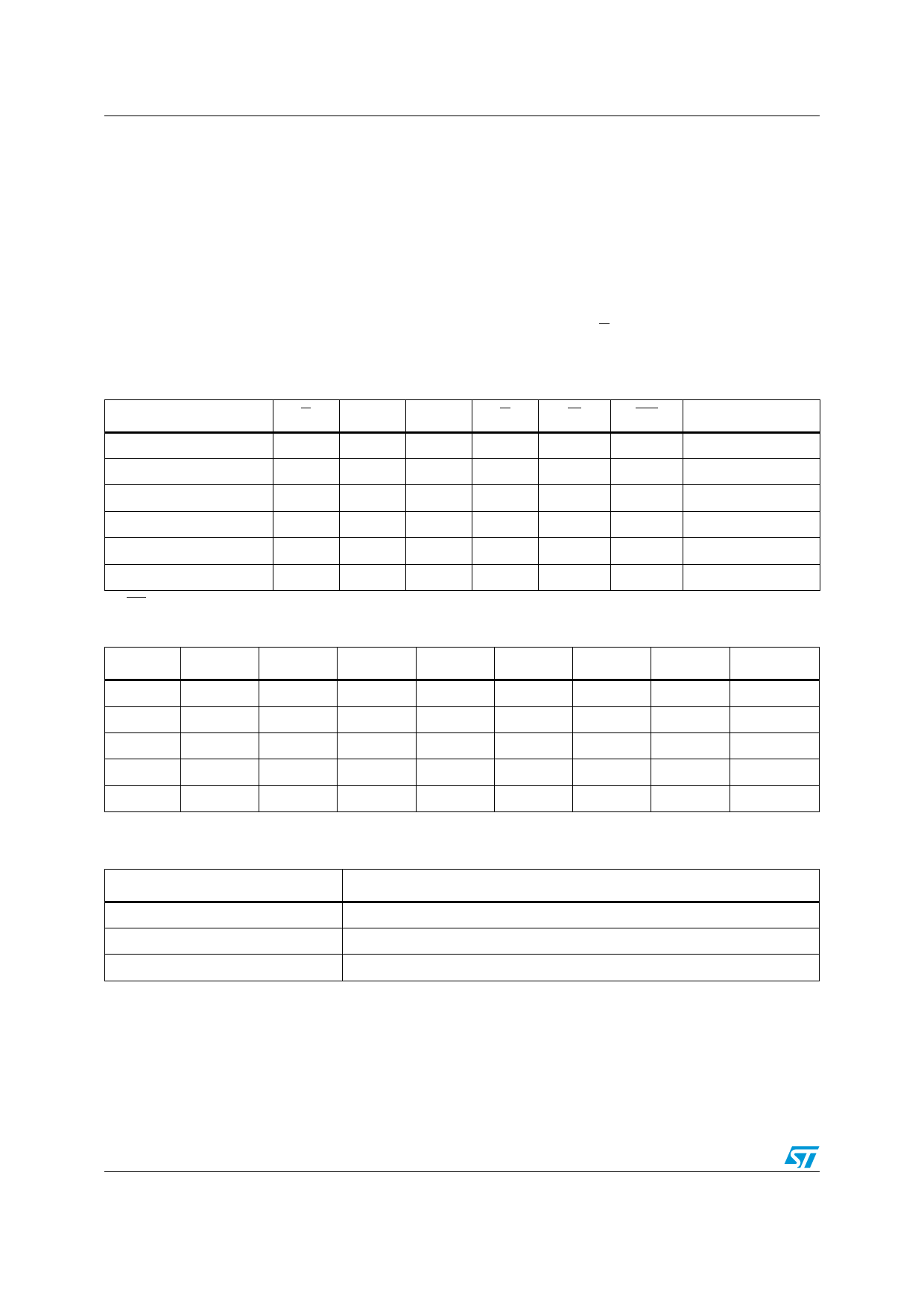
Table 5. Bus Operations
Bus Operation
E
AL
CL
R
W
WP
I/O0 - I/O7
Command Input
Address Input
Data Input
Data Output
Write Protect
VIL
VIL
VIH
VIL
VIH
VIL
VIL
VIL
VIL
VIL
VIL
VIL
X
X
X
Standby
VIH
X
X
1. WP must be VIH when issuing a Program or Erase command.
Table 6. Address insertion(1)
VIH
VIH
VIH
Falling
X
X
Rising
Rising
Rising
VIH
X
X
X(1)
X
VIH
X
VIL
VIL/VDD
Command
Address
Data Input
Data Output
X
X
Bus Cycle I/O7
I/O6
I/O5
I/O4
I/O3
I/O2
I/O1
I/O0
1st
A7
A6
A5
A4
A3
A2
A1
A0
2nd
VIL
VIL
VIL
VIL
A11
A10
A9
A8
3rd
A19
A18
A17
A16
A15
A14
A13
A12
4th
A27
A26
A25
A24
A23
A22
A21
A20
5th
VIL
VIL
VIL
VIL
VIL
VIL
A29
A28
1. Any additional address input cycles will be ignored.
Table 7.
Address Definitions
Address
A0 - A11
A12 - A18
A19 - A29
Definition
Column Address
Page Address
Block Address
16/51
Share Link: 