NAND04GW3C2N1E データシートの表示(PDF) - STMicroelectronics
部品番号
コンポーネント説明
メーカー
NAND04GW3C2N1E Datasheet PDF : 51 Pages
| |||
6 Device operations
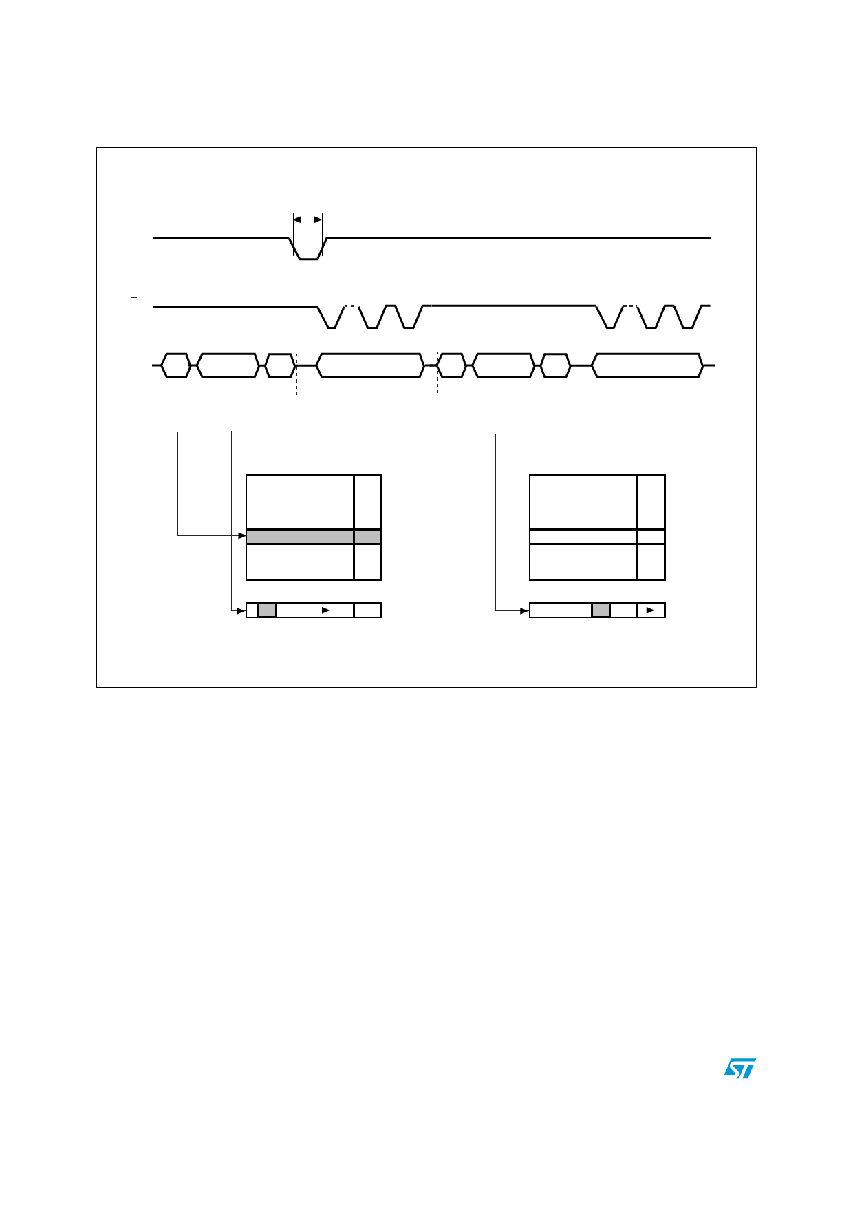
Figure 6. Random Data Output
NAND04GA3C2A, NAND04GW3C2A
tBLBH1
(Read Busy time)
RB
Busy
R
I/O
000h
Address
Inputs
30h
Cmd
Cmd
Code
Code
5 Add cycles
Row Add 1,2,3 Col Add 1,2
Main Area
Data Output
Spare
Area
05h
Address
Inputs
E0h
Cmd
Code
2Add cycles
Col Add 1,2
Cmd
Code
Data Output
Main Area
Spare
Area
ai08658b
6.4
Cache Read
The Cache Read operation is used to improve the read throughput by reading data using
the Cache Register. As soon as the user starts to read one page, the device automatically
loads the next page into the Cache Register.
An Cache Read operation consists of three steps (see Table 8):
1. One bus cycle is required to setup the Cache Read command (the same as the
standard Read command).
2. Five bus cycles are then required to input the Start Address (refer to Table 6).
3. One bus cycle is required to issue the Cache Read confirm command to start the P/E/R
Controller.
The Start Address must be at the beginning of a page (Column Address = 000h, see Table
7.). This allows the data to be output uninterrupted after the latency time (tBLBH1), see
Figure 7.
20/51
Share Link: 