NAND04GW3C2N1E データシートの表示(PDF) - STMicroelectronics
部品番号
コンポーネント説明
メーカー
NAND04GW3C2N1E Datasheet PDF : 51 Pages
| |||
NAND04GA3C2A, NAND04GW3C2A
5
Command Set
5 Command Set
All bus write operations to the device are interpreted by the Command Interface. The
Commands are input on I/O0-I/O7 and are latched on the rising edge of Write Enable when
the Command Latch Enable signal is high. Device operations are selected by writing
specific commands to the Command Register. The two-step command sequences for
program and erase operations are imposed to maximize data security.
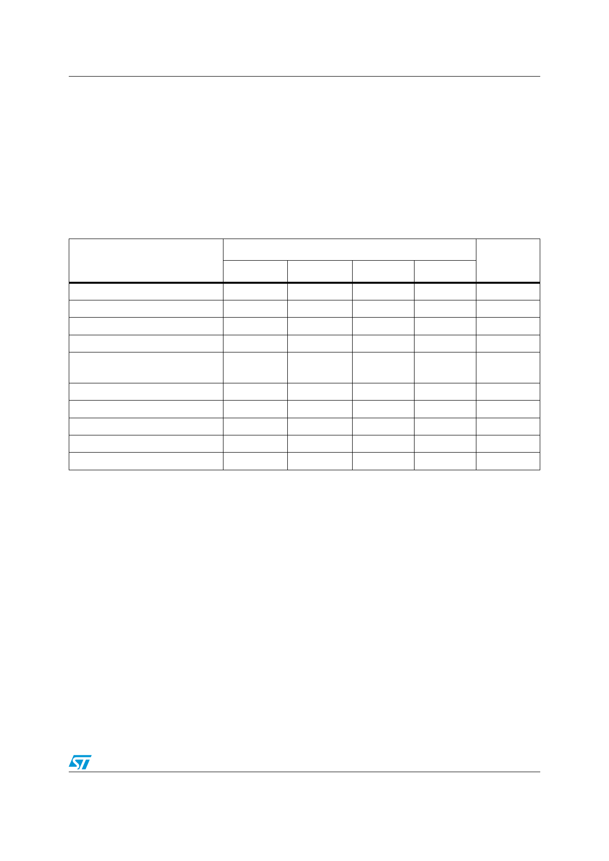
The Commands are summarized in Table 8: Commands.
Table 8. Commands
Command
1st CYCLE
Bus Write Operations(1)
2nd CYCLE 3rd CYCLE
4th CYCLE
Commands
accepted
during busy
Read
00h(2)
30h
–
–
Random Data Output
05h
E0h
–
–
Cache Read
Exit Cache Read
00h
31h
–
34h
–
–
–
–
Yes(3)
Page Program
(Sequential Input default)
80h
10h
–
–
Random Data Input
85h
–
–
–
Block Erase
60h
D0h
–
–
Reset
FFh
–
–
–
Yes
Read Electronic Signature
90h
–
–
–
Read Status Register
70h
–
–
–
Yes
1. The bus cycles are only shown for issuing the codes. The cycles required to input the addresses or input/output data are
not shown.
2. For consecutive read operations the 00h command does not need to be repeated.
3. Only when a Cache Read operation is ongoing.
17/51
Share Link: 