MT28S4M16B1LLFG-10 гГЗгГЉгВњгВЈгГЉгГИгБЃи°®з§ЇпЉИPDFпЉЙ - Micron Technology
йГ®еУБзХ™еПЈ
гВ≥гГ≥гГЭгГЉгГНгГ≥гГИи™ђжШО
гГ°гГЉгВЂгГЉ
MT28S4M16B1LLFG-10 Datasheet PDF : 58 Pages
| |||
BURST TYPE
Accesses within a given burst may be programmed
to be either sequential or interleaved; this is referred to
as the burst type and is selected via bit M3.
The ordering of accesses within a burst is deter-
mined by the burst length, the burst type, and the
starting column address, as shown in Table 1.
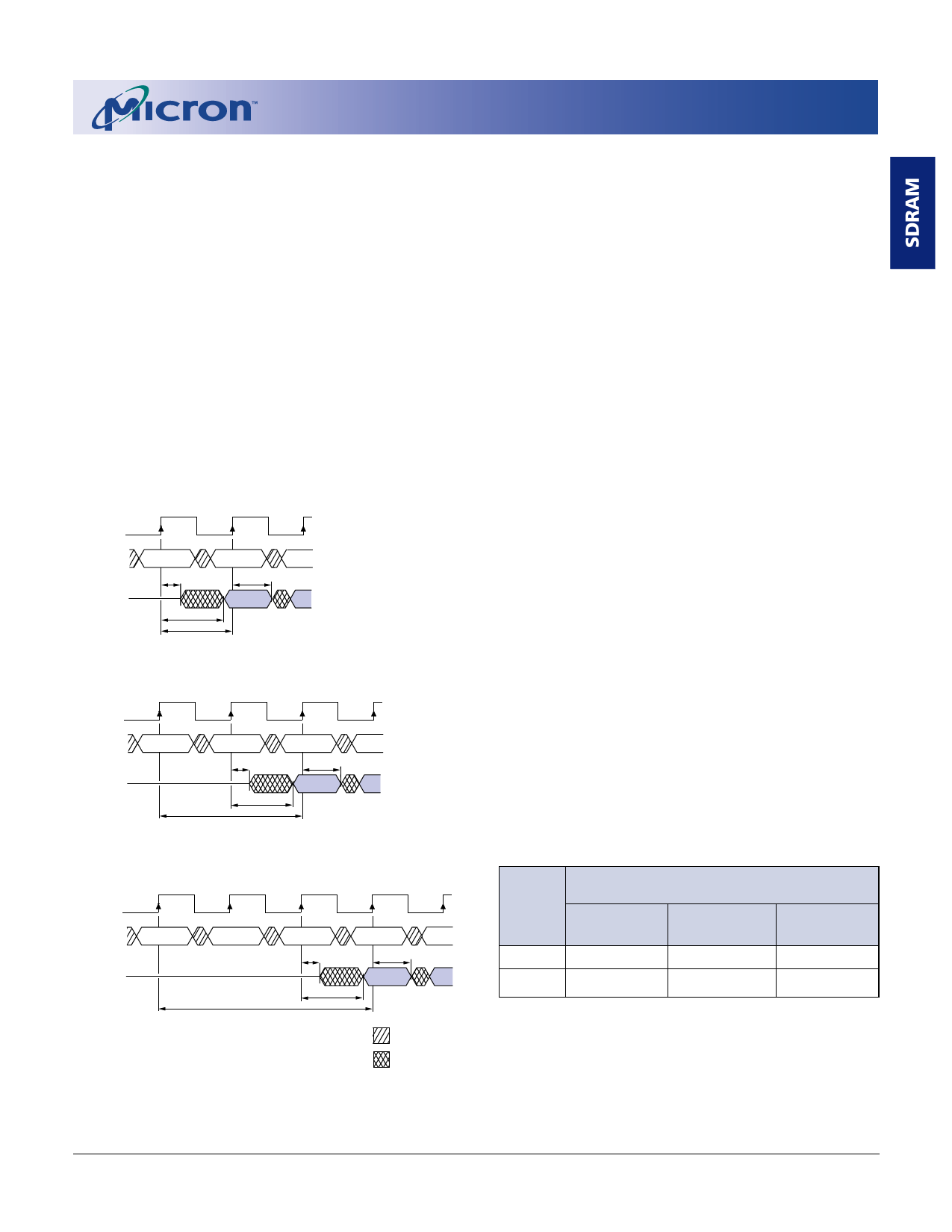
CAS LATENCY
The CAS latency is the delay, in clock cycles, be-
tween the registration of a READ command and the
availability of the first piece of output data. The la-
tency can be set to one, two, or three clocks.
Figure 2
CAS Latency
T0
T1
T2
CLK
COMMAND
DQ
READ
tLZ
tAC
NOP
tOH
DOUT
CAS Latency = 1
T0
T1
T2
T3
CLK
COMMAND
DQ
READ
NOP
tLZ
tAC
CAS Latency = 2
NOP
tOH
DOUT
CLK
COMMAND
T0
READ
DQ
T1
T2
NOP
NOP
tLZ
tAC
CAS Latency = 3
T3
T4
NOP
tOH
DOUT
DONвАЩT CARE
UNDEFINED
ADVANCE
64Mb: x16, x32
SYNCFLASH MEMORY
If a READ command is registered at clock edge n,
and the latency is m clocks, the data will be available by
clock edge n + m. The DQs will start driving as a result of
the clock edge one cycle earlier (n + m - 1), and provided
that the relevant access times are met, the data will be
valid by clock edge n + m. For example, assuming that
the clock cycle time is such that all relevant access times
are met, if a READ command is registered at T0 and the
latency is programmed to two clocks, the DQs will start
driving after T1 and the data will be valid by T2, as
shown in Figure 2. Table 2 indicates the operating fre-
quencies at which each CAS latency setting can be used.
Reserved states should not be used, as unknown
operation or incompatibility with future versions may
result.
OPERATING MODE
The normal operating mode is selected by setting M7
and M8 to zero; the other combinations of values for M7
and M8 are reserved for future use and/or test modes.
The programmed burst length applies to READ and
WRITE bursts (full-page burst WRITE not supported).
Test modes and reserved states should not be used
because unknown operation or incompatibility with
future versions may result.
WRITE BURST MODE
When M9 = 0, the burst length programmed via
M0вАУM2 applies to both read and write bursts; however,
if full-page burst length is selected in conjunction with
M9 = 0, the burst write length is 8 words for the x16 and
8-Dwords for the x32 (not full page). When M9 = 1, the
programmed burst length applies to READ bursts, but
write accesses are single-location (nonburst) accesses.
Table 2
CAS Latency
SPEED
-8
-10
ALLOWABLE OPERATING
FREQUENCY (MHz)
CAS
CAS
CAS
LATENCY = 1 LATENCY = 2 LATENCY = 3
£50 MHz
£100 MHz
£125MHz
£40 MHz
£83 MHz
£100 MHz
64Mb: x16, x32 SyncFlash
MT28S4M16B1LL.p65 вАУ Rev. 1, Pub. 5/02
11
Micron Technology, Inc., reserves the right to change products or specifications without notice.
©2002, Micron Technology, Inc.
Share Link: 